
Merry Christmas and a Happy New Year 2017 from LNAFIN Oy!
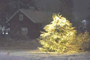
With this Christmas card our Best Wishes to All!
Many thanks for all our customers and for our collegues from behalf of LNAFIN Oy, Helsinki, Finland!
Many thanks for all our customers and for our collegues from behalf of LNAFIN Oy, Helsinki, Finland!
Blogi-sivuja päivitetään aktiivisesti tällä hetkellä vain englanniksi.
LNAFIN Oy:n blogi-sivuilla on uutisia, kehitystiedotteita sekä videoita tuotteistamme ja palveluistamme kuten piirilevyistä, PCB suunnittelusta, PCB kokoonpanosta ja R&D palveluista.
Julkaistut suunnittelutiedot ovat joko meidän omista R&D-projekteistamme, tai ne ovat julkaistu asiakkaan suostumuksella.

LNAFIN Oy Blog pages have news, development notices and videos about our products and services such as PCB Layout Design, RF-MMIC design and advanced PCB products and services. You can read the posts directly below, or access them via the categories listed above. The Q-band LNA category includes posts about our Q-band LNA MMIC design project for the European Space Agency (ESA), whereas Technical category includes LNAFIN Oy PCB layout and other design articles, our patent information etc.
Published design data is either from our own R&D projects, or it has been included with customer permission.

 LNAFIN Oy osallistuu Alihankinta 2016 Messuille
Alihankinta 2016 kuuluu kansainvälisten messujen parhaimmistoon Suomessa. Teollisuuden alihankkijat ovat kokooontuneet Tampereelle vuosikausia saadaakseen näkyvyyttä, uusia yrityskontakteja ja tuoreita ideoita. Alihankinta-messut pidetään vuosittain Tampereen Messu- ja Urheilukeskukseen, Ilmailunkatu 20, 33900 Tampere. Tänä vuonna messuille osallistuu 1000 näytteilleasettajaa 20 maasta. Tästä johtuen näytteasetetut tuotteet ja palvelut ovat uskomattoman monelta eri tuotealueelta. Kuitenkin päätuotealueet voidaan luokitella seuraavasti: tuotantomenetelmät, tuotteet ja komponentit, R&D ja suunnittelupalvelut sekä ICT. Siksi meistä tuntuu, että LNAFIN Oy:n tuotteet ja palvelut voisivat kiinnostaa Alihankinta 2016 messuvieraita. Me tarjoamme: PCB suunnittelua, PCB toimitukset, elektroniikan ladontaa, R&D palveluita, lankabondauspalveluita, prototyyppi- ja RF suunnittelua.
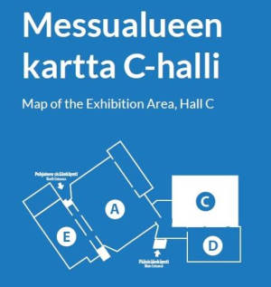
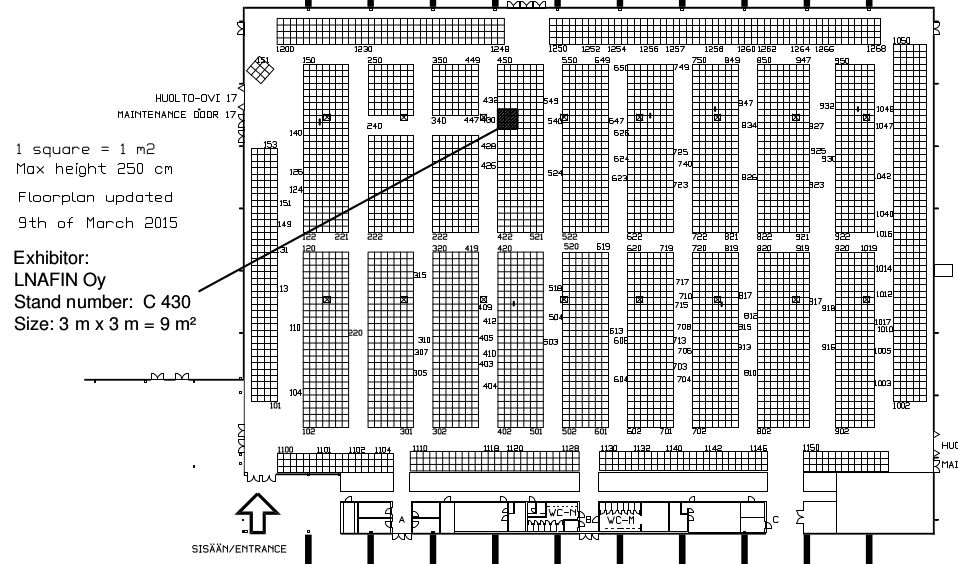
Tapaat meidät C-hallista osastolta C430. Olemme erittäin tyytyväisiä saatuamme oman osaston tästä tänä vuonnakin loppuunmyydystä tapahtumasta. Samalla toivomme, että mahdollisimman monella messuvieraalla olisi mielenkiintoa elektroniikka tuotteisiin ja suunnittelupalveluihin. Juttelemme mielellämme piirisuunnitteluun ja piirilevyihin liittyvistä prototyypitys/tuotantotarpeista. Kaikki osastokävijät voivat osallistua pieniin messuarpajaisiimme. Palkinnoiksi arvomme lahjakortteja tuotteisiimme. Voittajille ilmoitetaan henkilökohtaisesti ja voittajien nimet julkaistaan tässä blogissa. Olemme liittäneet tähän kirjoitukseen on kaksi opaskarttaa: sininen kartta näyttää koko messualueen kartan, ja allaoleva mustavalkoinen kartta kuvaa C-hallia. Meidän C 430 osastomme on selvästi merkitty karttaan.
Alihankinta 2016 is the foremost international industry trade fair in Finland. Industrial subcontractors have been gathering to Tampere for years to gain visibility, new business contacts and new ideas. The Alihankinta fair is held annually in Tampere Exhibition and Sports Centre, Ilmailunkatu 20, 33900 Tampere, Finland. This year’s fair has attracted 1000 exhibitors from 20 countries. As a result of that, the exhibited products and services vary tremendously. However, Alihankinta Fair main product categories have been categorized as: production methods, products and components, R&D and design services plus ICT. Thus we feel that LNAFIN Oy PCB layout design, PCB deliveries, electronics assembly, R&D services, wirebonding, prototyping and RF design know-how has something to offer for Alihankinta 2016 visitors.
You will meet us in C-hall at our booth C430. We are very satisfied to have gotten a booth in this year’s outsold event. At the same time we wish that many fair goers would have an interest in electronics products and design services. We would be pleased to discuss circuit design and printed circuit board related prototyping/production needs. All booth visitors can take part in our small fair lottery. We will randomly draw winners to receive gift certificates for our products. Winners will be personally informed. We have included two maps of the area in this post: the blue map above shows the general exhibition area layout, whereas the black-and-white map below shows the C-hall exhibitor map.
LNAFIN Oy Trademark Registration Celebrates Exports to 6 Countries WorldwideTo celebrate our starting sixth year in business, we have registered our trademark (TM) at the Finnish Patents and Trademark office. Our trademark LNAFIN cube logo is shown here with the famous circled R-letter. Its basic idea is to combine words LNA and FIN in a graphic form. LNA stands for Low-Noise Amplifier, which is a key block in most radio systems. We have one US patent on LNA structures. As for FIN: that stands for Finland. LNAFIN Oy operates from Helsinki, Finland, and we also wanted to give credit to great Finnish RF and electronics engineers.
Growing customer base has been one of the key reasons for TM regisration. This Spring our export destination count reached 6 different countries such as: USA, Russia, Denmark, Great Britain etc. We appreciate our customers’ trust very much and we will live up to it in the future too. We have delivered various printed circuit board related products such as PCB design, PCB sales and electronics assembly services.
Updated 2016 version of the LNAFIN Oy company slides has been posted here, or the .pdf file can be directly downloaded here.

 Sprint PCB layout design program is useful for the printed circuit designer who wants to layout designs directly without schematic entry or any such complexities. This simple productive tool offers professional PCB layout capabilities such as design reuse etc. and is thus very popular both in professional and hobbyist circles. In recognition of that, LNAFIN Oy has decided to start accepting native sprint files for PCB deliveries. These can also be used for prototype and series PCB assembly services when good Bill-of-Materials (BOM) is also included in the zip-file.
LNAFIN Oy has long supported several PCB layout programs such as: Mentorgraphics PADS, Eagle, and KiCAD. PCB layout design services are also available using these tools as based on customer schematic files. The Sprint data format complements our previously supported express-PCB PCB production in the sense that both tools focus on layout-only PCB approach. Here’s the Sprint quick logo for those who recognize that better:

We have relocated to bigger office space in Helsinki Hermanni area. The place is conveniently located as it lies at a 3 km distance from both the Helsinki Main and the Pasila Railway stations. Moreover, the drive to the Helsinki-Vantaa International Airport takes only 19 minutes.
New address: Orioninkatu 4, 00550 Helsinki, Finland.
Please note that the PO.Box 28 address we previously had for mail has been closed!
All mail should be send to our office in Orioninkatu.